
PCB Design

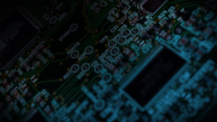
In order to make our design efficient, compact and reliable, we designed a PCB board to house all our hardware components together. This includes the power management system, sensor circuitry, microcontroller circuitry, SD card and FTDI circuitry.
Each component in the design is linked with actual parts found in the market and hence, the PCB was designed to scale. Also, each component has a footprint which shows the design of the component and gives the designer an indication of how it can be arranged effectively in the schematic shown above.
To view each circuit in detail please click here.
The Many Benefits using Altium CircuitMaker
The figure on the right shows the 3D view of a single component (SHTC3) in the PCB design. This is an example of one of many such components used in the circuit to make the different parts of the project. While some of the component footprints were pre-designed and acquired from SnapEDA or Altium's circuit vault, there were some that required to be manually designed to meet the manufacturer part specifications.

Placing the Order
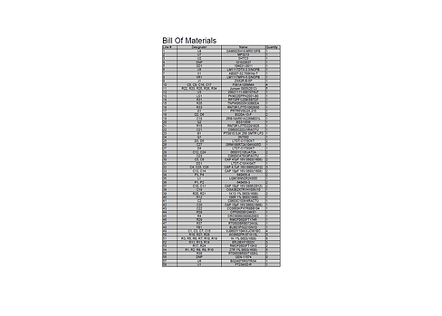
Finally, once the PCB design was completed, the parts were listed together in a tabular format called the Bill of Materials or BOM. The parts which weren't available were replaced with alternate ones with similar specifications and design, and were then sent out along with the design to the PCB manufacturing vendor, PCBWay, to acquire the board.
All Done!
The PCB board generally arrives with all parts soldered, but sometimes there are a few parts that are designated as DNP or 'do not place' in order to solder them in a specific way. Also, in our case, we have a touch sensor and a pulse sensor which need to be freely maneuverable in order to bring them close to the patient. These parts were not added to the PCB board and were attached separately to the PCB with the help of connectors.
